Nanofabrication
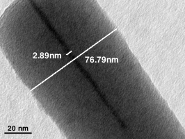
Continually pushing the boundaries of science and technology requires an endless search for novel and high utility nanofabrication techniques. Through the advanced lithography, masking, etching, and processing techniques we have developed, we regularly produce structures with lateral dimensions as small as 2nm, fabricate devices exhibiting aspect ratios of 60:1, and explore new device geometries using sophisticated 3-dimensional etch control. We have exploited these techniques to create sub-10nm diameter silicon structures capable of light emission, lithographically-defined quantum dots for tunable resonant tunneling devices, and suspended membranes with nanometer scale pores for biological sensing and characterization. Our research laboratory is built around producing such nanostructures and applying them to new optoelectronic, biomedical, and quantum-confined electronic devices, enabling higher speeds, greater efficiencies, as well as scientific investigation and technological integration in ways previously unachievable.