A new technique achieves precise localization of quantum dots into photonic crystal cavities [2]
Coherent coupling between a single quantum emitter and a spatially localized photon mode can lead to many intriguing opportunities in the context of various quantum electrodynamics experiments including a single photon source and a thresholdless laser. For successful demonstration of such an effect on a miniaturized chip scale, the state-of-the-art semiconductor nanofabrication technique and epitaxial technique should be combined together. Today, this requirement is often achieved by the use of PhC nanocavities and quantum dots (QDs) grown in a strain-induced self-assembled manner. [1]
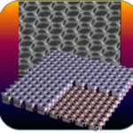
Here, we propose a simple and efficient method to create QDs through post-processing a quantum well (QW) layer, which takes an advantage of a unique topological characteristic of a PhC [2]. More specifically, the method involves the formation of quantum-size emitters within a pre-defined PhC in a self-aligned fashion through controlled removal of a QW layer via selective wet-chemical etching. In fact, the idea of processing an epitaxially grown QW to obtain QDs dates back to 1980s [3]. The best available technology at that time enabled an array of etched nano-pillars whose lateral dimension goes down to ~40 nm. However, this method inevitably removes most of the bulk semiconductor, which might pose additional technological challenge as to how a useful optical resonator can be implemented along with the QDs fabricated in this way. Our new method indeed solves this issue and further provides several feasible plans for 1D, 2D, and 3D PhCs.
As preliminary experiments, we successfully fabricate vertically stacked QDs well-aligned with respect to the PhC backbone. Micro-photoluminescence measurements performed at 78K reveal that the radiative transition energy blue-shifts as the lateral dimension reaches below 50 nm, which agrees well with a simple model based on the ‘particle-in-a-box’ picture and the Wannier exciton theory.
The proposed method may find a broad range of applications in photonics and quantum optics, where the coupling between an emitter and an optical mode needs to be maximized. Using the proposed method, an active quantum nanostructure can be precisely located with respect to a given high-Q optical cavity. Isolation of an active region will be of crucial importance when making electrically-pumped nanolasers in the context of efficient current confinement. Moreover, the partitioning between an active region and a passive region will improve the performance of a nanolaser by quenching unwanted re-absorption of generated photons. More importantly, passive waveguides can be easily integrated on the same chip without relying on much more complex methods involving epitaxial re-growth. This active/passive integrated structure can allow efficient in- and out-coupling of photons from a wavelength-small photon source.
References
- Yoshie, T., Scherer, A., Hendrickson, J., Khitrova, G., Gibbs, H. M., Rupper, G., Ell, C., Shchekin, O. B., & Deppe, D. G. (2004). Vacuum Rabi Splitting with a Single Quantum Dot in a Photonic Crystal Nanocavity. Nature, 432(7014), 200-203.
- Oh, D., Kim, S.-H., Huang, J., Scofield, A., Huffaker, D. & Scherer, A. (2013). Self-Aligned Quantum Nanostructures in Photonic Crystals via Selective Wet-Chemical Etching. Nanotechnology, 24(26), 265201.
- Kash, K., Scherer, A., Worlock, J. M., Craighead, H. G. & Tamargo, M. C. (1986). Optical Spectroscopy of Ultrasmall Structures Etched from Quantum Wells. Applied Physics Letters, 49(16), 1043-1045.