A new class of photonic crystal cavities in optically thick slabs [2]
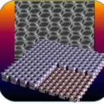
A thin dielectric membrane with periodically perforated air-holes – known as a photonic crystal (PhC) slab – has provided a versatile platform for high-Q optical resonators and waveguides that are confined by the photonic bandgap. Since the invention of the PhC slab in the early 1990, there was established a consensus in the community as to the proper thickness (T) of the PhC slab that T should be around λ/2neff in order to optimize the size of the photonic bandgap. For example, for the design of a PhC resonator working at a wavelength of 1300 nm, this thickness consideration suggests T ~ 200 nm (assuming InP/InGaAsP material systems). Such optically-thin slab systems have enabled many interesting results including high-Q > 1 million with a wavelength-small mode volume < (λ/neff)3. However, we would like to note that the very thickness requirement of T = λ/2neff also placed a severe constraint on the design of current-injection PhC nanolasers.
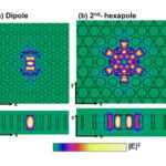
Now we are revolutionizing the design of PhC nanocavities, by rebutting the old concept and/or proposing a new class of optically-thick PhC slabs. As for the first one [1] in our thick-slab-work series, we have theoretically studied a very thick PhC slab (T up to 2~3 µm) and found that it can support sufficiently high-Q (few thousands) modes for lasing. Experimentally, we have successfully achieved a lasing at about 1300 nm from the PhC dipole mode in a thick slab with T = 606 nm [Fig. 1(a)]. However, this PhC dipole mode emits more photons into the in-plane directions than into the vertical direction, which is not desirable for efficient photon collection. Moreover, even the theoretical highest Q could not exceed 3,000 in T = 606 nm. It would seem, at first, that we have no other options for further improvement in Q because the poor horizontal confinement appears inevitable due to the absence of a photonic bandgap.
In our recent publication [2], we pose the question of whether we can design a certain resonant mode emitting at 1300 nm that is confined by a photonic bandgap in a slab with T = 606 nm. The answer is yes and in the first part of the paper we provide the design of a second-order hexapole mode whose Q is about 15,000 and bounded by a tiny photonic bandgap at about λ=1365 nm [Fig. 1(b)]. Next, we perform intensive numerical simulations optimizing Q by varying various structural parameters. Such optimization processes inevitably break the condition of the photonic bandgap. Surprisingly, even in the absence of a photonic bandgap, a certain set of parameters gives Q of over 100,000 along with a fairly good horizontal confinement (hence the vertical extraction efficiency over 70%). Experimentally, we achieve single-mode lasing at 1347 nm from the designed second-order hexapole mode, by pulsed optical pumping at room-temperature. We believe that, by removing the thickness constraint of T = λ/2neff, many unconventional cavity designs which were previously discarded because they cannot support a photonic bandgap can now be reconsidered.
References
- Kim, S.-H., Huang, J. & Scherer, A. (2012). Photonic Crystal Nanocavity Laser in an Optically Very Thick Slab. Optics Letters, 37(4), 488-490.
- Kim, S.-H., Huang, J. & Scherer, A. (2013). Higher-Order Defect-Mode Laser in an Optically Thick Photonic Crystal Slab. Optics Letters, 38(2), 94-96.